const 发布的文章

“const”

raw socket编程。

运行第一段代码,发送ip数据报,第二段代码接收ip数据报。需要运行第二段代码,否则将无法接收数据报。

#include<stdio.h>
#include<string.h>
#include<stdlib.h>
#include<sys/socket.h>
#include<sys/types.h>
#include<netinet/in.h>
 
struct iphead{   
    unsigned char ip_hl:4, ip_version:4;  //ip_hl,ip_version各占四个bit位。
    unsigned char ip_tos;
    unsigned short int ip_len;   
    unsigned short int ip_id;
    unsigned short int ip_off;  
    unsigned char ip_ttl;
    unsigned char ip_pro;
    unsigned short int ip_sum;
    unsigned int ip_src;
    unsigned int ip_dst;
};
 
struct icmphead{  //该结构体模拟ICMP报文首部
    unsigned char icmp_type;
    unsigned char icmp_code;
    unsigned short int icmp_sum;
    unsigned short int icmp_id;
    unsigned short int icmp_seq;
};
 
unsigned short int cksum(char buffer[], int size){   //计算校验和,具体的算法可自行百度,或查阅资料
    unsigned long sum = 0;
    unsigned short int answer;
    unsigned short int *temp;
    temp = (short int *)buffer;
    for( ; temp<buffer+size; temp+=1){
        sum += *temp;
    }
    sum = (sum >> 16) + (sum & 0xffff);
    sum += (sum >> 16);
    answer = ~sum;
    return answer;
}
 
int main(){
   
    int sockfd;
    struct sockaddr_in conn;
    struct iphead *ip;
    struct icmphead *icmp;
    unsigned char package[sizeof(struct iphead) + sizeof(struct icmphead)];  //package存储IP数据报的首部和数据
    memset(package, 0, sizeof(package));
 
    ip = (struct iphead*)package;
    icmp = (struct icmphead*)(package+sizeof(struct iphead)); //IP数据报数据字段仅仅包含一个ICMP首部
    sockfd = socket(AF_INET, SOCK_RAW, IPPROTO_ICMP); //创建套接字
    if(sockfd < 0){
        printf("Create socket failed\n");
        return -1;
    }
    conn.sin_family = AF_INET;
    conn.sin_addr.s_addr = inet_addr("192.168.230.135");
    int one = 1;
    if(setsockopt(sockfd, IPPROTO_IP, IP_HDRINCL, &one, sizeof(one)) < 0){  //设置套接字行为,此处设置套接字不添加IP首部
        printf("setsockopt failed!\n");
        return -1;
    }
    /*设置IP首部各个字段的值*/  
    ip->ip_version = 4; 
    ip->ip_hl = 5;
    ip->ip_tos = 0;
    ip->ip_len = htons(sizeof(struct iphead) + sizeof(struct icmphead)); //关于htons()、htonl()的作用,可自行百度    
    ip->ip_id = htons(1);
    ip->ip_off = htons(0x4000);
    ip->ip_ttl = 10;
    ip->ip_pro = IPPROTO_ICMP;
    ip->ip_src = htonl(inet_addr("192.168.230.135"));
    ip->ip_dst = htonl(inet_addr("192.168.230.135"));
    printf("ipcksum : %d\n", cksum(package, 20)); 
    ip->ip_sum = cksum(package, 20);  // 计算校验和,应当在其他字段之后设置(实验中发现检验和会被自动添加上)
    
    /*设置ICMP首部各字段值*/
    icmp->icmp_type = 8;
    icmp->icmp_code = 0;
    icmp->icmp_id = 1;
    icmp->icmp_seq = 0;
    icmp->icmp_sum = (cksum(package+20, 8));
    /*接下来发送IP数据报即可*/
    if(sendto(sockfd, package, htons(ip->ip_len), 0,(struct sockaddr *)&conn, sizeof(struct sockaddr)) < 0){
    printf("send failed\n"); 
    return -1;
    }
    printf("send successful\n");    
    return 0;
}

第二段程序

#include <stdio.h>
#include <string.h>
#include <stdlib.h>
#include <sys/socket.h>
#include <sys/types.h>
#include <netinet/in.h>
#include <unistd.h>
#include <linux/if_ether.h>

unsigned short int cksum(char buffer[], int size){  //校验函数
    unsigned long sum = 0;
    unsigned short int answer;
    unsigned short int *temp;
    temp = (short int *)buffer;
    for( ; temp<buffer+size; temp+=1)
        sum += *temp;
    sum = (sum >> 16) + (sum & 0xffff);
    sum += (sum >> 16);
    answer = ~sum;
    return answer;
}

int main(){
    unsigned char buffer[1024];
    
  //  int sockfd = socket(AF_INET, SOCK_RAW, IPPROTO_ICMP);//不知为啥,无法设置原始套接字在网络层抓IP数据报
    int sockfd = socket(PF_PACKET, SOCK_RAW, htons(ETH_P_IP)); //此处,利用原始套接字在数据链路层抓取MAC帧,去掉
    if(sockfd < 0){                                            //14个字节的MAC帧首部即可
        printf("create sock failed\n");
    return -1;
    }    
    int n = recvfrom(sockfd, buffer, 1024, 0, NULL, NULL); //接收MAC帧

    printf("receive %d bytes\n", n);
    for(int i=14; i<n; i++){      //去掉MAC帧首部,直接输出IP数据报每个字节的数据
    if((i-14) % 16 == 0)
        printf("\n");
    printf("%d ",buffer[i]);
    }
    printf("\n");
    printf("ipcksum: %d\n", cksum(buffer+14, 20)); //此处再次校验时,应当输出0
    return 0;
}

这是之前参考
Referenced from:https://blog.csdn.net/nice_wen/article/details/53416063

SIO 包含哪些功能?

虽不同款芯片支持的功能可能不尽相同,但是大体流程和基本功能还是很相近的,下面以Nct6106D为例:

LPC总线,原名叫Low Pin Count Bus,是在IBM PC兼容机中用于把低带宽装置,连接到CPU上。这些低速设备有:BIOS,Super I/O,TPM。LPC总线通常和主板上的南桥物理相连。 LPC总线是Intel在1998时作为工业标准架构体系(ISA)的替代品引入,它与ISA在软件层面是类似的,尽管在物理层面有着巨大不同,ISA是16bit宽,8.33 MHz的总线,而它是4bit宽,有着四倍频率(33.3 MHz)的总线。 

FDC: FOLPPY DISK CONTROLLER,软盘控制器.
PRT: PARALLEL PORT, 也称打印机接口逻辑.
UART: Universal Asynchronous Receiver/Transmitter, 标准异步收发器,俗称串口.
KBC: KEYBOARD CONTROLLRT, 键盘控制器, PS/2.
CIR: CONSUMER INFRARED REMOTE , 谷歌翻译为:消费者红外遥控器,暂时没用过,猜测是一种红外传感器吧.
GPIO: General Purpose Input Output.通用型输入输出.
GPIO,WDT: WatchDog Timer, 支持一个8位可编程的超时计数器.ACPI: 简称电源管理, 信号连接到南桥(7A芯片组),用于将系统从S1~S5唤醒睡眠状态.
others: 包含SmartFan,Led等功能,就不详细说了.
这款芯片虽然集成了好多功能,但是使用有限,加之之前调试过几个常用功能,那我们就摘之为例进行详细介绍:

如何通过Lpc来初始化SIO?

SIO,按照手册来讲,不单单支持LPC接口,也支持SMBUS,那么如果我们将SIO接到LPC总线上,我们如何控制它呢?

1.他作为一个IO设备,我们需要通过LpcIo的方式进行通讯,在龙芯处理器,Lpc的Io物理地址->虚拟地址(0x18000000->0xefdfc000000,通过X1Bar配置窗口映射到HT1的IO空间),所以LpcIo的访问我们使用UNCACHE_ADDR(0xefdfc000000)).2.通过SIO芯片控制逻辑进行功能选择:AccessSio逻辑图与代码逻辑如下:
在这里插入图片描述
VOID
Nct6106d_write(

   UINT8 dev,                                                                                                    
   UINT8 addr,                                                                                                   
   UINT8 data)                                                                                                   

{

/*enter*/                                                                                                       
outb(BONITO_PCIIO_BASE_VA + OFFSET_2E_4E + 0x002e,0x87);                                                        
if(dev != 0xff)                                                                                                 
{                                                                                                               
/*select logic dev reg */                                                                                       
outb(BONITO_PCIIO_BASE_VA + OFFSET_2E_4E + 0x002e,0x7);                                                         
outb(BONITO_PCIIO_BASE_VA + OFFSET_2E_4E + 0x002f,dev);                                                         
}                                                                                                               
/*access reg */                                                                                                 
outb(BONITO_PCIIO_BASE_VA + OFFSET_2E_4E + 0x002e,addr);                                                        
outb(BONITO_PCIIO_BASE_VA + OFFSET_2E_4E + 0x002f,data);                                                        
/*exit*/                                                                                                        
outb(BONITO_PCIIO_BASE_VA + OFFSET_2E_4E + 0x002e,0xaa);                                                        

}
12345678910111213141516171819202122

相信大家也都看明白了,如果你是一名软件人员,在这里有个注意的,那就是需要查看硬件原理图来确定究竟是0x2E,0x2F,还是0x4E,0x4F的端口.这是硬件的地址引脚来决定的.
上图代码中的dev标志着SIO内的逻辑设备控制器,addr是逻辑设备控制器内offset

设备ID对照表:
在这里插入图片描述

Global Control register的操作方式我们已经在代码中以dev=0xff的形式进行了区分,你在上图中应该已经发现.

Global Controller Register

简单介绍一下该组控制寄存器,以代码为例:

                                                                                             
Nct6106d_write(0xff,0x02,0x01);//reset                                                                                                                                                                        
Nct6106d_write(0xff,0x26,0xc3);//2e_4e                                                                                                                                                                        
Nct6106d_write(0xff,0x29,0xff);//disable legacy mode                                                                                                                                                          
Nct6106d_write(0xff,0x1a,0x00);//ps/2                                                                                                                                                                         
Nct6106d_write(0xff,0x1c,0x1e);//uart                                                                                                                                                                                                                                                                                                                                                                      

123456

0x02: Reset SIO 寄存器0x1a: MutliFunc 引脚复用寄存器,举例:如若使用PS/2,那么首先就需要将对应引脚设置为PS/2的功能.
其他寄存器就先不详细说了,简单上图0x1a举例:
在这里插入图片描述

UART Func

UART就不多介绍了,异步通讯收发器: 我们俗用串口输出调试,也有一些产品上将之作为串行打印机,串行鼠标键盘等.
Nct61061d这款芯片共集成了6个UART控制器,UARTA~UARTF.
访问UARTA见下图SIO手册及代码:
在这里插入图片描述

//Nct6106d_UARTA                                                                                                
Nct6106d_write(2,0x30,0x01);                                                                                    
Nct6106d_write(2,0x60,0x03);                                                                                    
Nct6106d_write(2,0x61,0xf8);                                                                                    
Nct6106d_write(2,0x70,0x4);                                                                                     
Nct6106d_write(2,0xf0,0x2);

1234567

配置流程:

1 通过0x30将UARTA进行功能Enable
2 通过0x60,0x61将UARTA的该组寄存器映射到LpcIo的地址端口上,比如配置的0x3f8,那么如果我们想要访问UART控制器组的话,就需要通过UNCACHE_ADDR(0xefdfc000000+0x3f8)进行访问了,关于UART寄存器组都是按照协议规范定义的,可以正常使用标准协议驱动.
3 通过0x70,我们来分配该UARTA的中断号. 在龙芯平台上, 中断号0-15已经分配给了Lpc下面的设备哦.
4 通过0xf0,可以对UARTA进行时钟分频.
先写到这里,关于UARTA的配置及SIO的详细寄存器组我相信或多或少都有了解,所有的功能都大同小异,通过Lpc配置SIO,每款SIO芯片可能Access逻辑稍有区别,但是SIO内部的逻辑设备符合标准驱动模型.
有关该款Nct6106d的芯片手册见资源下载.nct6102d_nct6106d_datasheet_v1_0.pdf

Referenced from:https://blog.csdn.net/weixin_45384176/article/details/114579738

SB = standby
ACPI有以下几种模式:
S0 正常。 S1 CPU停止工作。 S2 CPU关闭。 S3 除了内存外的部件都停止工作。 S4 内存信息写入硬盘,所有部件停止工作。 S5 关闭。
CMOS中大多有一个[Power Savings]选项,可选[Maximum Battery Life]或Maximum Performance等。设置节能选项时,主要设置由idle Mode进入Standby Mode的[Standby Timeout]的时间和由[Standby Mode]进入[Suspend Mode]的Suspend Timeout的时间

5VSB由ATX电源提供的待机电压,然后通过主板上的电子电路多级转换得到3VSB,1V8SB,1V5SB,!V2SB等待机电压,电压分别为3.3V,1.8V,1.5V,1.2V等。

示例:
GPIO4 Group
Enable: Logic Device 7, CR30[4]
Data: Logic Device 7, F0~F3
Multi-function: YLW, GRN, PLED, SMI (Logic Device 8, CRE4[7-0])
Reset: Logic Device 9, CRE2[4]
OD/PP: Logic Device F, CRE4
Name Pin Default function Default type GPIO power plane Switch default function to GPIO
GP40 40 GP40 input 3VSB
GP41 41 GP41 input 3VSB
GP42 42 GP42 input 3VSB
GP43 43 GP43 input 3VSB
GP44 44 GP44 input 3VSB
GP45 45 GP45 input 3VSB
GP46 46 GP46 input 3VSB
GP47 47 GP47 input 3VSB

On different operation system, have different method to read/write I/O port. I
know WinIO on windows, IoWrite8/16/32 on Linux.

There is a good open source software “Open Hardware Monitor”, which develop by
C# language. It support almost all the motherboard.

  1. Datasheet of chipsLook the access channels on file NCT6776F_NCT6776D_Datasheet_V1_2
    page 275

19.2 ACCESS CHANNELS
There are two different channels to set up/access the GPIO ports. The first one is the indirect access via register
2E/2F (4E/4F, it depends by HEFRAS trapping). The registers can be read / written only when the respective
logical device ID and port number are selected.
known that rigister index is 0x2E, and data Input/Output port is 0x2F

On page 54

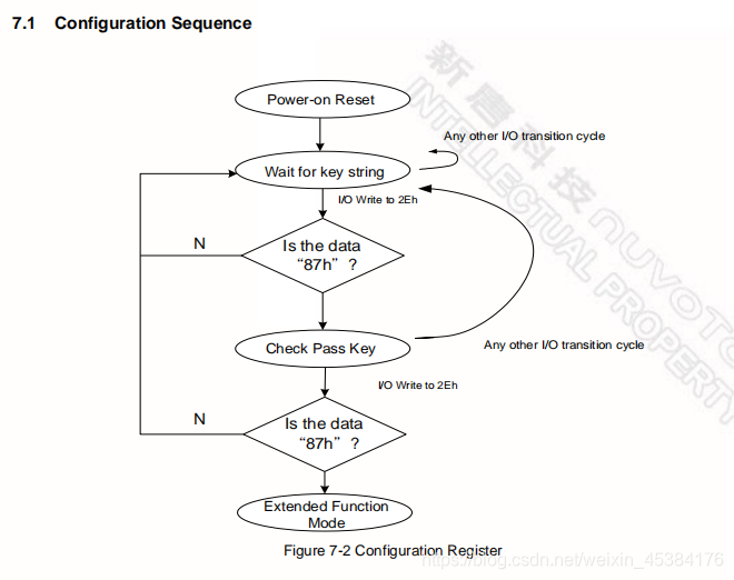
To program the NCT6776F / NCT6776D configuration registers, the following configuration procedures must be
followed in sequence:
(1). Enter the Extended Function Mode.
(2). Configure the configuration registers.
(3). Exit the Extended Function Mode.

7.1.1 Enter the Extended Function Mode
To place the chip into the Extended Function Mode, two successive writes of 0x87 must be applied to Extended
Function Enable Registers (EFERs, i.e. 2Eh or 4Eh).

7.1.2 Configure the Configuration Registers
The chip selects the Logical Device and activates the desired Logical Devices through Extended Function Index
Register (EFIR) and Extended Function Data Register (EFDR). The EFIR is located at the same address as the
EFER, and the EFDR is located at address (EFIR+1).
First, write the Logical Device Number (i.e. 0x07) to the EFIR and then write the number of the desired Logical
Device to the EFDR. If accessing the Chip (Global) Control Registers, this step is not required.

Secondly, write the address of the desired configuration register within the Logical Device to the EFIR and then
write (or read) the desired configuration register through the EFDR.

7.1.3 Exit the Extended Function Mode
To exit the Extended Function Mode, writing 0xAA to the EFER is required. Once the chip exits the Extended
Function Mode, it is in the normal running mode and is ready to enter the configuration mode.
Software Programming Example
The following example is written in Intel 8086 assembly language. It assumes that the EFER is located at 2Eh, so
the EFIR is located at 2Eh and the EFDR is located at 2Fh. If the HEFRAS (CR[26h] bit 6 showing the value of
the strap pin at power on) is set, 2Eh can be directly replaced by 4Eh and 2Fh replaced by 4Fh.
This example programs the configuration register F0h (clock source) of logical device 1 (UART A) to the value of
3Ch (24MHz). First, one must enter the Extended Function Mode, then setting the Logical Device Number (Index
07h) to 01h. Then program index F0h to 3Ch. Finally, exit the Extended Function Mode.

;-----------------------------------------------------
; Enter the Extended Function Mode
;-----------------------------------------------------
MOV DX, 2EH
MOV AL, 87H
OUT DX, AL
OUT DX, AL
;-----------------------------------------------------------------------------
; Configure Logical Device 1, Configuration Register CRF0
;-----------------------------------------------------------------------------
MOV DX, 2EH
MOV AL, 07H
OUT DX, AL
; point to Logical Device Number Reg.
MOV DX, 2FH
MOV AL, 01H
OUT DX, AL
; select Logical Device 1
;
MOV DX, 2EH
MOV AL, F0H
OUT DX, AL
; select CRF0
MOV DX, 2FH
MOV AL, 3CH
OUT DX, AL
; update CRF0 with value 3CH
;-----------------------------------------------
; Exit the Extended Function Mode
;----------------------------------------------
MOV DX, 2EH
MOV AL, AAH
OUT DX, AL

  1. Open Hardware MonitorHomepage
  2. code

The Open Hardware Monitor is a free open source software that monitors
temperature sensors, fan speeds, voltages, load and clock speeds of a computer.

As below, introduct how to use VC++ to monitor HW status on windows:

1). modify computer.cs,add some interface like GetFanSpeed(). if have problem , look report function .
2). set the project properity to output class library.
3). Reference VC++ use C# DLL

1.1 Analyze open-hardware-monitorUse Winbond W83627DHG-P chip as example.

A description about how to monitor hardware, see this
http://www.supermicro.com/support/faqs/faq.cfm?faq=12015

Question
I'm trying to access the Winbond 83627DHG-P IO chip on the motherboard X8SIL.
We want to use the LMsensor. Do you have the offset codes for the smbus?

Answer
Bus Type = ISAIO/SMBus
One W83627DHG-P

Windbond W83627DHG-P, Slave Address=0x2d (0x5a in 8-Bit format)

OR IndexReg=A15, DataReg=A16

Fan1 Fan Speed, Bank 0, Offset 0x29 RPM = 1350000/8/Data
Fan2 Fan Speed, Bank 5, Offset 0x53 RPM = 1350000/8/Data
Fan3 Fan Speed, Bank 0, Offset 0x28 RPM = 1350000/8/Data
Fan4 Fan Speed, Bank 0, Offset 0x3f RPM = 1350000/8/Data
Fan5 Fan Speed, Bank 0, Offset 0x2a RPM = 1350000/8/Data

CPU Voltage, Bank 0, Offset 0x20 Voltage = Data* 0.008
-12V Voltage, Bank 0, Offset 0x26 Voltage = ((Data*0.008-2.048)/(10./242.))+2.048
+12V Voltage, Bank 0, Offset 0x21 Voltage = Data* 0.008/ (10./66.2)

AVCC Voltage, Bank 0, Offset 0x22 Voltage = Data* 0.016
3.3Vcc Voltage, Bank 0, Offset 0x23 Voltage = Data* 0.016

DIMM Voltage, Bank 0, Offset 0x24 Voltage = Data* 0.008
+5V Voltage, Bank 0, Offset 0x25 Voltage = Data* 0.008/ (10./40.)
+3.3VSb Voltage, Bank 5, Offset 0x50 Voltage = Data* 0.016

VBAT Voltage, Bank 5, Offset 0x51 Voltage = Data* 0.016

CPU Temperature, Bank 1, Offset 0x50 Temperature = Data

System Temperature, Bank 2, Offset 0x50 Temperature = Data

Chassis Intrusion, Bank 0, Offset 0x42, BitMask 0x10 1 = Bad, 0 = Good
(Clear Bit: Bank 0, Offset 0x46, BitMask 0x80)

Power Supply Failure, GP23(From W83627DHG-P) 1 = Good, 0 = Bad

1.1.1 File: Hardware/LPC/LPCIO.csIO Ports

// I/O Ports
private readonly ushort[] REGISTER_PORTS = new ushort[] { 0x2E, 0x4E };
private readonly ushort[] VALUE_PORTS = new ushort[] { 0x2F, 0x4F };
Winbond, Nuvoton, Fintek

private const byte FINTEK_VENDOR_ID_REGISTER = 0x23;
private const ushort FINTEK_VENDOR_ID = 0x1934;

private const byte WINBOND_NUVOTON_HARDWARE_MONITOR_LDN = 0x0B;

private const byte F71858_HARDWARE_MONITOR_LDN = 0x02;
private const byte FINTEK_HARDWARE_MONITOR_LDN = 0x04;

private void WinbondNuvotonFintekEnter() {
Ring0.WriteIoPort(registerPort, 0x87);
}

private void WinbondNuvotonFintekExit() {
Ring0.WriteIoPort(registerPort, 0xAA);
}
ITE

private const byte IT87_ENVIRONMENT_CONTROLLER_LDN = 0x04;
private const byte IT8705_GPIO_LDN = 0x05;
private const byte IT87XX_GPIO_LDN = 0x07;
private const byte IT87_CHIP_VERSION_REGISTER = 0x22;

private void IT87Enter() {
Ring0.WriteIoPort(registerPort, 0x87);
Ring0.WriteIoPort(registerPort, 0x01);
Ring0.WriteIoPort(registerPort, 0x55);
}

private void IT87Exit() {
Ring0.WriteIoPort(registerPort, CONFIGURATION_CONTROL_REGISTER);
Ring0.WriteIoPort(valuePort, 0x02);
}
SMSC

private void SMSCEnter() {
Ring0.WriteIoPort(registerPort, 0x55);
}

private void SMSCExit() {
Ring0.WriteIoPort(registerPort, 0xAA);
}
How to get value:call ReadByte to get value:

byte id = ReadByte(CHIP_ID_REGISTER);
byte revision = ReadByte(CHIP_REVISION_REGISTER);
look at function ReadByte:

private byte ReadByte(byte register) {
Ring0.WriteIoPort(registerPort, register);
return Ring0.ReadIoPort(valuePort);
}
first, write register value to registerPort;
second, read value from valueport.

1.1.2 File: Hardware/LPC/W836XX.csHow to get value:// Hardware Monitor
private const byte ADDRESS_REGISTER_OFFSET = 0x05;
private const byte DATA_REGISTER_OFFSET = 0x06;

// Hardware Monitor Registers
private const byte BANK_SELECT_REGISTER = 0x4E;

private byte ReadByte(byte bank, byte register) {
Ring0.WriteIoPort(

 (ushort)(address + ADDRESS_REGISTER_OFFSET), BANK_SELECT_REGISTER);

Ring0.WriteIoPort(

 (ushort)(address + DATA_REGISTER_OFFSET), bank);

Ring0.WriteIoPort(

 (ushort)(address + ADDRESS_REGISTER_OFFSET), register);

return Ring0.ReadIoPort(

(ushort)(address + DATA_REGISTER_OFFSET));

}
What is the value of “address”:set value by construction

public W836XX(Chip chip, byte revision, ushort address) {
this.address = address;
this.revision = revision;
this.chip = chip;
...
}
on LPCIO.cs, found the calling code:

private const byte BASE_ADDRESS_REGISTER = 0x60;

ushort address = ReadWord(BASE_ADDRESS_REGISTER);

switch (chip) {
case Chip.W83627DHG:
case Chip.W83627DHGP:
case Chip.W83627EHF:
case Chip.W83627HF:
case Chip.W83627THF:
case Chip.W83667HG:
case Chip.W83667HGB:
case Chip.W83687THF:

superIOs.Add(new W836XX(chip, revision, address));
break;

...
}
Get temperature:private readonly byte[] TEMPERATURE_REG = new byte[] { 0x50, 0x50, 0x27 };
private readonly byte[] TEMPERATURE_BANK = new byte[] { 1, 2, 0 };

for (int i = 0; i < temperatures.Length; i++) {
int value = ((sbyte)ReadByte(TEMPERATURE_BANK[i],

TEMPERATURE_REG[i]))  0) 
value |= ReadByte(TEMPERATURE_BANK[i],
  (byte)(TEMPERATURE_REG[i] + 1)) >> 7;

float temperature = value / 2.0f;
if (temperature = -55 && !peciTemperature[i]) {

temperatures[i] = temperature;

} else {

temperatures[i] = null;

}
}
Get fan speed:call ReadByte(FAN_TACHO_BANK[i], FAN_TACHO_REG[i]) to get speed value to “count”
, then set real fan spee to array variable “fans[]“.

private readonly byte[] FAN_TACHO_REG =
new byte[] { 0x28, 0x29, 0x2A, 0x3F, 0x53 };
private readonly byte[] FAN_TACHO_BANK =
new byte[] { 0, 0, 0, 0, 5 };
private readonly byte[] FAN_BIT_REG =
new byte[] { 0x47, 0x4B, 0x4C, 0x59, 0x5D };
private readonly byte[] FAN_DIV_BIT0 = new byte[] { 36, 38, 30, 8, 10 };
private readonly byte[] FAN_DIV_BIT1 = new byte[] { 37, 39, 31, 9, 11 };
private readonly byte[] FAN_DIV_BIT2 = new byte[] { 5, 6, 7, 23, 15 };

ulong bits = 0;
for (int i = 0; i < FAN_BIT_REG.Length; i++)

bits = (bits > FAN_DIV_BIT2[i]) & 1) > FAN_DIV_BIT1[i]) & 1) > FAN_DIV_BIT0[i]) & 1));
int divisor = 1  192 && divisorBits < 7) 
    divisorBits++;
if (count < 96 && divisorBits > 0)
    divisorBits--;

newBits = SetBit(newBits, FAN_DIV_BIT2[i], (divisorBits >> 2) & 1);
newBits = SetBit(newBits, FAN_DIV_BIT1[i], (divisorBits >> 1) & 1);
newBits = SetBit(newBits, FAN_DIV_BIT0[i], divisorBits & 1);

}

Referenced from:https://matrix207.github.io/2012/12/17/monitor-hardware-status/

'Re: Implement a watchdog' - MARC
update:2021-11-9

i have a ENDAT 7703 motherboard near my desk,
the manual point out some instruction to configure the
watchdog :

//init, select the destination of command...

outportb(0x2e,0x87);
outportb(0x2e,0x07);
outportb(0x2f,0x08);

//com

outportb(0x2e,0x30); //main

outportb(0x2f,0x01); //0 to inactive

outportb(0x2e,0xf2); //reset param

outportb(0x2f,0x00); // bit 6 keyboard, bit 7 mouse

outportb(0x2e,0xf0); //time unit conf
outportb(0x2f,0x04); // bit3 = 1 minutes

outportb(0x2e,0xf1); // how much time
outportb(0x2f,1); // 1 minute

I suppose only the kernel can write to the 0x2e and 0x2f address ?

Usually watchdog are detected and shown in dmesg, have i to ask more
detail to the supplier ?

Looks like a semi-standard "motherboard plug and play" SuperIO unlock
sequence to me. If you can find out what chip they use on the
motherboard, you might be able to find a data sheet for it.

Referenced from:https://marc.info/?l=openbsd-tech&m=141821845915978&w=2